
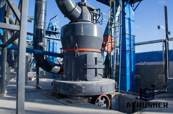
wafer back grinding services malaysia manufacturer Grasping strong production capability, advanced research strength and excellent service, Shanghai wafer back grinding services malaysia supplier create the value and bring values to all of customers.
 WhatsApp)
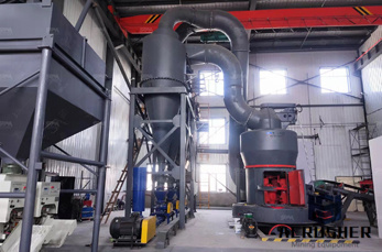
WLP Services; Wafer Backside Metallization; Pac Tech offers high quality wafer back metallization process including back grinding and stress relief with TiNiAg qualified for PowerMOSFET and other devices. E-beam evaporation technology. PacTech Asia uses an e-beam evaporation technology for its wafer backside metallization. ...
Wafer Thinning. There are four primary ways to thin wafers, (1) mechanical grinding, (2) chemical mechanical planarization, (3) wet etching and (4) atmospheric downstream plasma dry chemical etching (ADP DCE).There are two groups that make up the four wafer thinning techniques: grinding .
Wafer Back Grinding Tapes. ... Wafers requiring grinding and thinning to 50 microns needs high performance adhesion and yet easily release on demand either by UV or heat curing. AIT wafer and substrate grinding and thinning temporary bonding adhesive tapes are made in the United States with Company Service Centers in China and USA. The high ...
Leading-edge CMP, wafer thinning and wafer polishing solutions.
Back grinding is a process that removes silicon from the back surface of a wafer. Silicon Valley Microelectronics provides grinding on our own substrates or on customer supplied wafers. We process bare and device patterned wafers with high yield and offer wafer thinning to customer specifications. SVM Wafer Back Grinding Capabilities:
Contacts page classic with contact form in HTML. grinding machine jobs in malaysia. We sincerely welcome you to contact us through hotlines and other instant communication ways.
Wafer Backgrind Wafer Backgrind is the process of grinding the backside of the wafer to the correct wafer thickness prior to assembly. It is also referred to as 'wafer thinning.' Wafer backgrinding has not always been necessary, but the drive to make packages thinner and thinner has made it indispensable.
13 hours ago· Press release - KD Market Insights - Wafer Backgrinding Tape Market Volume Analysis, Segments, Value Share and Key Trends 2019-2026 - published on openPR
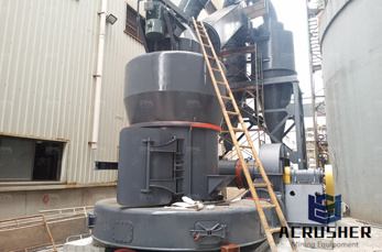
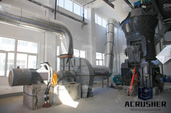
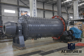
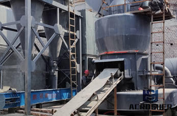
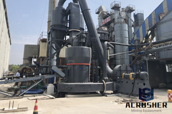
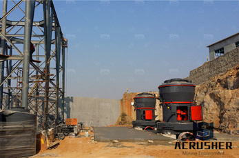
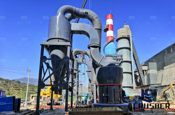
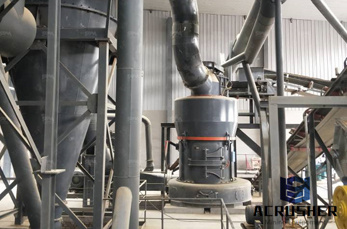
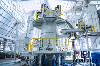
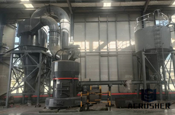
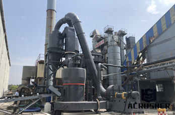
back grinding machines in semiconductor Our Purpose And Belief L&M Heavy Industry is committed to provide the global customers with the first-class products and superior service, striving to maximize and optimize the interests and values of the customers, and build bright future with high quality.
In order to meet industry demands for turnkey WLCSP products, TF-AMD has offered the service from Wafer Probing and Wafer Back grind as well. TF-AMD use fully-automated wafer back grinding equipment to achieve high level of quality for post grind wafer. The process includes wafer backgrinding, die singulation, AOI and packing in tape & Reel.
Wafer Services PVD and Dicing: Home Products Contact Assembly Wire Bonders Wafer PVD Vapor Deposition and wafer dicing services Available from these companies: Listed Alphabetically: Country: Address : Contact: PVD Coating Films: Back Grinding: Dicing: USA: American Dicing 7845 Maltlage Dr
Mar 06, 2014· iX-factory has in-depth expertise in wafer dicing. The video shows the process of wafer dicing in the state-of-the-art facilities of iX-factory.
In this process, a UV-curable adhesive is applied to wafer surfaces and used as a bonding agent between glass support substrates and wafers. Grinding stresses on the wafer are minimized as the adhesive flows into and supports the topography of the circuit patterns on the front side of the wafers.
The LINTEC Adwill series includes UV curable dicing tapes, high performance back grinding tapes, dicing die bonding tapes required for semiconductor packaging, and backside coating tapes. Adwill continues to make steady progress in the advancement of related equipment and unique systems.
Syagrus Systems uses the 3M Wafer Support System to meet the demands of today's technology companies for extremely thin silicon wafers and die used in complex applications. We have over 15 years of silicon wafer thinning and wafer backgrinding experience, including bumped wafer backgrinding and have provided wafer backgrind services since 1997. ...
Grinding and Dicing Services, complete resource for Wafer Polishing, Grinding, Dicing,Plating, Back grinding,Dye SLevel Thinning in San Jose. GDSI Wafer Polishing. As packages begin to shrink and become more flexible, so must the die that go in them. GDSI has developed a polishing process that relieves the stress induced by grinding while ...
POREX ® Tubular Membrane Filter (TMF)™ Applied in Die Saw Wastewater Reclaim System for a Microelectronics Company in Shenzhen, China. Introduction. Die sawing and backgrinding are processes which are used to cut large silica wafers into smaller discs. After either of these processes, the wafer chips must be rinsed with Ultrapure Water (UPW) to remove fine silica particles and any other ...
Wafer Preparation services are offered as part of your turnkey packaging and assembly project or as stand-alone services based on your individual needs. With our advanced wafer processing equipment, Quik-Pak offers expert backgrinding services for wafer-level packaging. We can take your wafers and backgrind to expose heat sinks, anodes ...
Quik-Pak, originally founded in 1994 as SPT, was purchased by Delphon Industries in 2000. For the last 15 years, Quik-Pak has provided fast turn IC Packaging, Assembly, Prototype and Wafer Processing Services to a wide variety of Semiconductor and Electronics Companies, as well as major Military and Aerospace institutions.
TAIKO is a DISCO developed wafer back grinding method. By enabling an outer support ring to the wafer (the TAIKO ring, Japanese for drum), back grinding is performed on the inner circular area of the wafer, while leaving an edge of a few millimeters unprocessed. Taiko simplifies thin wafer .
Wafers thinned down to 75 to 50 μm are common today. Prior to grinding, wafers are commonly laminated with UV-curable back-grinding tape, which ensures against wafer surface damage during back-grinding and prevents wafer surface contamination caused by infiltration of grinding .
Wafer Level Packing services, Pac Tech Asia provides a complete turnkey solution especially for PowerMOSFET products, including front metallization (E-less NiAu/ NiPdAu plating), back grinding, back metallization, dicing and die sorting. Wafer Thinning and Backmetal Specifications Wafer Thinning Wafer
PDF | Ultrathin silicon wafer technology is reviewed in terms of the semiconductor applications, critical challenges, and wafer pre-assembly and assembly process technologies and their underlying ...
GDSI, Grinding and Dicing Services complete resource for Silicon Wafers Processing includes Probing, Bumping, Grinding, Polishing in San Jose, California. Back Grinding Services by Silicon Valley Microelectronics, Inc. (SVM). Back grinding is a process that removes silicon from the back surface of a wafer.
WhatsApp)