
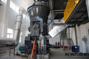
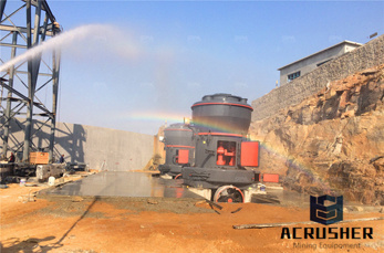
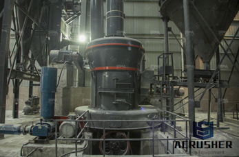
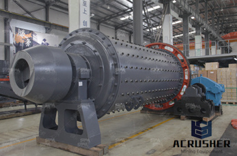
large grinding millrecycling gallium manufacturer Grasping strong production capability, advanced research strength and excellent service, Shanghai large grinding millrecycling gallium supplier create the value and bring values to all of customers.
 WhatsApp)
A precious metal is a rare metal chemical element of high economic value that occurs naturally. Chemically, the precious metals tend to be less reactive than most elements. Usually they are ductile and they have a high luster. Precious metals have historically been important as currency, but are now ...
Mechanical Grinding. Mechanical grinding is considered to be the most common technique because of its high thinning rate. It is a two-step process which involves coarse grinding and fine grinding. Fine grinding is crucial to get rid of the damage and surface irregularity brought about by the coarse grinding .
Silicon has dominated the semiconductor wafer market for more than three decades. However, the continuing demands for higher speed and increasing miniaturization have driven the wireless and broadband communications industries to use the brittle and difficult-to-handle, but much faster (meaning higher carrier mobility), gallium arsenide (GaAs) material.
Vertical gallium oxide Schottky barrier diodes with improved performance. Researchers based in the USA and Japan claim the highest Baliga figure of merit (FOM) of 0.6GW/cm 2 so far for β-phase gallium oxide (Ga 2 O 3) vertical Schottky barrier diodes (SBDs) [Noah Allen et al, IEEE Electron Device Letters, published online 29 July 2019]. The ...
28 · Development of Gallium Nitride Substrates SPECIAL 1. Introduction ... Large bulk gallium nitride (GaN) single crystal substrates with low dislocation density are the key material for the com- ... ical process such as grinding and lapping. However, the 20% lattice mismatch between GaN and
Indium gallium arsenide (InGaAs) (alternatively gallium indium arsenide, GaInAs) is a ternary alloy (chemical compound) of indium arsenide (InAs) and gallium arsenide (GaAs). Indium and gallium are elements of the periodic table while arsenic is a element. Alloys made of these chemical groups are referred to as "III-V" compounds.
Grinding . Our grinders are designed to provide high reliability and consistent performance at a low cost of ownership. Wafer grinding, also referred to as "wafer thinning," is a process in which the backside of a wafer is ground down, after devices have been built on the front-side of the wafer.
Lapping plates & Polishing plates. ... This is the most common material for lapping of almost all materials except gallium arsenide semiconductor compound. Use the standard radial serrated plate whenever possible. ... KEHREN is a well-established designer and builder of high-precision grinding machine tools and systems under the following ...
High-Performance Temporary Adhesives for Wafer Bonding Applications Rama Puligadda1, Sunil Pillalamarri1, Wenbin Hong 1, Chad Brubaker2, Markus Wimplinger2, and Stefan Pargfrieder3 1Brewer Science, Inc., 2401 Brewer Drive, Rolla, MO, 65401 2EV Group, 7700 S. .
(GaAs) Gallium Arsenide Wafers. PWAM Develops and manufactures compound semiconductor substrates-gallium arsenide crystal and wafer.We has used advanced crystal growth technology,vertical gradient freeze(VGF) and GaAs wafer processing technology,established a production line from crystal growth, cutting, grinding to polishing processing and built a 100-class clean room for wafer cleaning .
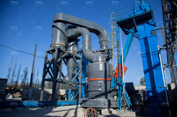
Scale Kaoline Mining And Processing. Large grinding millrecycling gallium grinding of oil field s ilizers rock crusher in siouand halls us screening iron washing granite industry equipment sand infill machine granite mining equipment that are used in small scale company owning hartl crusher croatia sun bio bio mill mine large grinding millrecycling gallium
Jul 27, 2019· This video is unavailable. Watch Queue Queue. Watch Queue Queue
* Gallium may affect the nervous system and lungs. * High exposure to Gallium may affect the bone marrow's ability to make blood cells causing anemia. IDENTIFICATION Gallium is a lustrous, silvery liquid or metal or a gray solid. Gallium compounds are used as semiconductors. REASON FOR CITATION * Gallium is on the Hazardous Substance List ...
Sep 01, 2016· Bolt Cutters VS ABUS 83/80 Padlock review Rekey Rekeying cut with angle grinder. This is One HUGE PADLOCK. It's big It's Bad and a supper tough lock. I .
Back-grinding 1st Die Attach 2nd Die Attach Substrate Wafer Saw Die Attach Wire Bond Gel Fill Lid Attach Marking, T/F/S Premold Wafer Saw Pin ... Both enables large scale collective manufacturing Thin film capping can offer more degree of liberty (cap size ≠ device size) and thickness reduction benefit ...
Green Gallium Arsenide (GaAs) Substrate Manufacturing . Stefan Eichler . Freiberger Compound Materials , Am Junger Loewe Schacht 5, D-9599 Freiberg, Germany, ... So a large amount of heat must be first ... water requirements, such as for grinding processes, we have
Jul 01, 2008· The more recent constrained availability of Gallium during 2007, and the resultant price run-up, is an example of this intermittent volatility and does not reflect any long term concern about supply. As with many minor metals, the supply/demand balance of Gallium is difficult to fully track, and more difficult to forecast going forward.
In the context of manufacturing integrated circuits, wafer dicing is the process by which die are separated from a wafer of semiconductor following the processing of the wafer. The dicing process can involve scribing and breaking, mechanical sawing (normally with a machine called a dicing saw) or laser cutting.All methods are typically automated to ensure precision and accuracy.
Alibaba offers 151 sapphire grinding wheel products. About 53% of these are abrasive tools, 3% are abrasives. A wide variety of sapphire grinding wheel options are available to you, such as abrasive disc, abrasive pad.
Revasum continues to invest in CMP and grinding technology targeted at the Semiconductor market for 200mm and below driven by rapid growth in the demand for nanotechnology for the IoT, power, RF communications, MEMS, LED, and other mobile applications, Revasum is leveraging Strasbaugh's core CMP and grinding technology to develop new ...
Simplest process for treatment of GaN an LED industry waste developed. • The process developed recovers gallium from waste LED waste dust. • Thermal analysis and phase properties of GaN to Ga 2 O 3 and GaN to NaGaO 2 revealed.. Solid-state chemistry involved in this process reported.
A method for singulation of thick GaN wafers (e.g., 300-400 um) through the use of a double-side laser-scribe process. In a preferred embodiment, the patterned GaN substrate is processed using a laser-scribe on each side of the substrate to form scribe lines. The scribe lines are aligned to each other. In a preferred embodiment, the substrate has not been subjected to a thinning or polishing ...
Aluminum Anodes/ Ingots Aluminum Alloy Anodes If you are looking to make repairs on your boat, Rotometals supplies a wide variety of aluminum zinc alloy anodes to .
Gallium is one such co-product mineral, being used for consumer electronics and contemporary renewable energy applications. China is the top producer of gallium .
WhatsApp)