
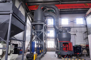
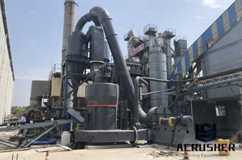
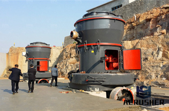
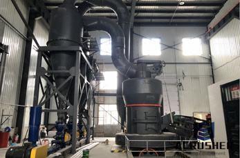
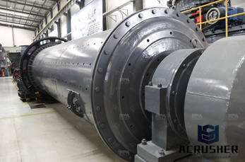
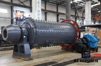
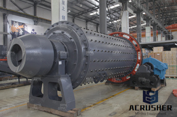
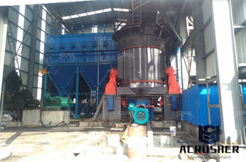
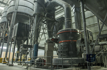
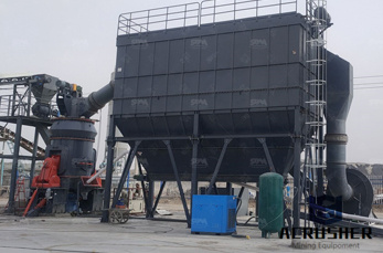
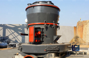
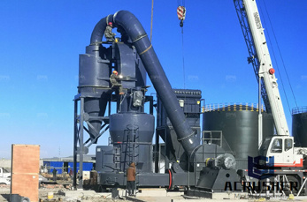
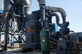
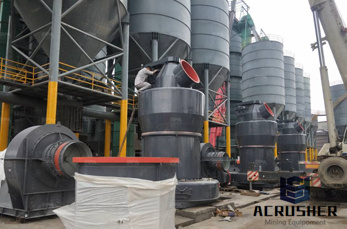
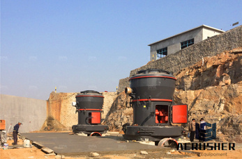
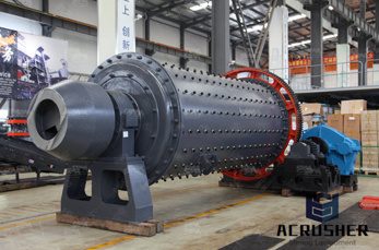
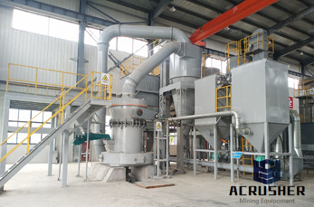
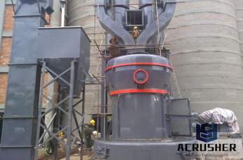
grinding process in mems manufacturer Grasping strong production capability, advanced research strength and excellent service, Shanghai grinding process in mems supplier create the value and bring values to all of customers.
 WhatsApp)
A SI-CMOS-MEMS process using back-side grinding - IEEE Xplore This paper presents a Si-CMOS-MEMS fabrication process which leaves the back-side silicon under the CMOS metal and oxide layers, and improves the ...
Back grinding is a process that removes silicon from the back surface of a wafer. Silicon Valley Microelectronics provides grinding on our own substrates or on customer supplied wafers. We process bare and device patterned wafers with high yield and offer wafer thinning to customer specifications. SVM Wafer Back Grinding Capabilities:
In the context of manufacturing integrated circuits, wafer dicing is the process by which die are separated from a wafer of semiconductor following the processing of the wafer. The dicing process can involve scribing and breaking, mechanical sawing (normally with a machine called a dicing saw) or laser cutting.
process the user may build their own process. Step 3 is to then select a fab to run the process in, a wide variety of MEMS fabs from around the world are already predefined and available for selection in a drop-down list. In step 4, up to 4 substrates per MEMS die are selected from drop-down lists for each MEMS process.
Quik-Pak, originally founded in 1994 as SPT, was purchased by Delphon Industries in 2000. For the last 15 years, Quik-Pak has provided fast turn IC Packaging, Assembly, Prototype and Wafer Processing Services to a wide variety of Semiconductor and Electronics Companies, as well as major Military and Aerospace institutions.
The ultrasonic vibration mill-grinding process can be considered as a combination of ultrasonic vibration machining process and mill-grinding process. As shown in Fig. 1(a), the grinding wheel's motion relative to workpiece in UVMG includes the rotation motion in .
Mar 06, 2014· iX-factory has in-depth expertise in wafer dicing. The video shows the process of wafer dicing in the state-of-the-art facilities of iX-factory.
MEMS, MOEMS, sensors and other devices will be designed and fabricated with Stealth technology as the preferred medium for final singulation or dicing. The addition of Stealth Laser Dicing services fortifies our line of mechanical saws, which has been the de facto dicing standard for decades.
Many substrate materials can benefit from one or several grinding process to rapidly remove material, correct or optimize shape, and even achieve target surface finishes that can eliminate downstream processes. Grinding solutions for electronics are offered in partnership with Saint-Gobain Abrasives (Norton and Winter). Grinding Products
Failure modes of Wafer Level Thin Film MEMS packages during wafer thinning. ... of the grinding process. ... thin film packaging process for a MEMS cantilever type resonator using a 4-mask ...
back-side silicon using back-side grinding. The Si-CMOS-MEMS process includes a grinding process followed by a bonding process and conventional post-CMOS etch. A Si-CMOS-MEMS accelerometer is used to demonstrate the feasibility of the Si-CMOS-MEMS process. A 0.2 µm flatness of ground silicon surface over 2 mm length is achieved in this work.
Grinding Process In Mems . A SICMOSMEMS PROCESS USING BACKSIDE GRINDING metal and oxide layers and improves the uniformity of the backside silicon using backside grinding The The SiCMOS MEMS process includes a grinding process . A Prehensive Review Of Microgrinding Emphasis On . Microgrinding is a tool based mechanical micromachining process ...
In MEMS devices blade dicing is largely applied for singulating the ASIC, capping and MEMS sensors. However, exposure to water from the process can contaminate some sensors and destroy sensitive MEMS structures, example in MEMS microphones. In such cases, stealth dicing has been already adopted in large volume production.
Although largely unknown in the MEMS community, micromachining using ultrasonic impact grinding (UIG) is a fascinating yet easy fabrication scheme to achieve virtually any shape, such as a shallow or deep reservoir, a channel, a via, etc, in silicon, glass and other commonly used ceramic and semiconductor materials in the MEMS field.
The thickness variation and the breakage of silicon diaphragms are mainly dictated by the grinding process, since grinding forces may deflect the diaphragm leading to non-uniform material removal within the cavity area. The thickness variation is largest at the centre of the cavity and decreases towards the edge of the cavity.
Products/Services for MEMS Grinding Polishing Buffs and Buffing Wheels - (105 companies) Buffs and buffing wheels are used to hold finishing compounds and polish parts made of metal, plastic, ceramic, glass, wood, stone, silicon, or optical materials.
In addition, boundary layer effects may distort contamination readings due to ineffective sensor designs. The invention presents a novel sensor design for in-situ heavy metal detection, while resolving boundary layer problems to achieve extremely sensitive detection rates.
MEMS packaging accounts for 20-60% of the MEMS device BOM and is a key part of the MEMS function and design Packaging creates additional value as the MEMS device is integrated into a system (SiP, module) Standardization enables high volume production (second sourcing, cost efficiency through technology sharing)
Abstract. Dissolved wafer process (DWP) is being extensively used to fabricate complex micro-electro-mechanical system (MEMS) structures. Etching non-uniformity, increased surface roughness and duration of DWP is often influence MEMS devices yields.
The thinning of wafers is called grinding. As a rule, the grinding process takes place in several steps, each with a finer grain of the grinding wheels. On the one hand, this serves to optimize the process duration and, on the other hand, to reduce the damage to the crystal caused by grinding in the crystal.
- Process Responsible for Grinding /wafer Thinning, Wafer Molding, Dry Film Resist (DFR ) lamination, Dicing/wafer saw, Edge Trim & Bonding processes Bonding & Assembly Process Development Process Engineer, MEMS - Dicing and Grinding Process
This application note discusses the Edge Grinding of hard, brittle materials that are common to semiconductor, MEMS, LEDs, and other applications. Edge grinding, also known as Edge Profiling, is a process that is common to the manufacture of nearly all semiconductor related
Philips Innovation Services operates a state-of-the-art 2650 m 2 pure-play MEMS Foundry on the High Tech Campus in Eindhoven, the Netherlands. This MEMS Foundry is specialized in low to medium volume custom MEMS manufacturing.
MEMS Dicing. Dicing takes a finished wafer (post-wafer fabrication) and converts it into individual dies; it's the step where the front-end fab process transitions to the back-end assembly process. Grinding & Dicing Services, Inc. has accumulated 25 years of engineering and process knowledge supporting semiconductor, consumer electronics, and ...
WhatsApp)